Electric/ Ceramic Circuit Board that Operation
Product Introduction
Substrate material
Tensky ceramic PCB is made up of innovative, research and development engineers the configuration, the target is the first leader professional Ceramic base plate, ceramic circuit board brought to workshop, using a semiconductor membrane technology for a customer with OEM/ODM service, Resolution, Customer in electronic circuit in various thermal heating, high pressure, and the problem.
Main materials:Al2O3 and AlN substrate.
Image layers metal:Ti, TiW, Cu , Ni, Pd , Au , Ag, AuSn, Sn, Al…and other metallize。
Primary market:high-power LED stand, cooling, optical communication components, optical power solar energy base plate, vehicle with electrical, air, and the electronic circuit board roadbed, and so on.
The special is high power LED market context, such as 1515, 2016, 3535, 5050, 6060, 1215 substrate, and LED - COB integrated stand, practices, as well as UVLED stand, etc. product is the Secretary's main work specifications, provide customer professional views, reduced customer test and failure risk.
Micro-resistive element has 0402,0603,0805,1206,2512 and other specifications 0 ohms to 3 ohms
applications, the main market for the 3C industry battery module market.
Film surface
 |
 |
 |
Metallized material / design
Substrate Materials
Material |
Typical thickness (mm) |
Typical dimension |
Thermal conductivity |
Al2O3 Wafer |
0.38/ 0.5 /0.635/0.8/1mm |
4.5" /5” |
20~27 W/mK |
Al2O3 Chip |
0.38/ 0.5 /0.635/0.8/1mm |
Customized |
|
AlN Wafer |
0.38/ 0.5 /0.635 |
4.5“/5” |
170~200 W/mK |
ALN Chip |
0.38/ 0.5 /0.635 |
Customized |
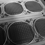
Wafer Drawing
Material |
Patternconstruction |
Laser drill for via-holes |
Laser scribing |
Line width for dicing saw |
Clearance distance from edge to metalized pattern |
Al2O3 Wafer |
Single Face |
80~200 um, |
1/4~1/2 |
150~300 um, |
6mm (as the thickness of the metalized layer less than 30 um); |
AlN Wafer |
|||||
Al2O3 Chip |
|||||
ALN Chip |